 “Zoom in.”
“A little more.”
“What evidence do you see in the surface appearance that you can use to determine if it is a brittle or ductile failure?”
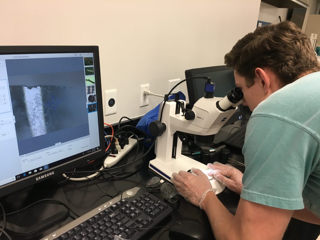
MSE Professor Nancy Ruzycki, Ph.D., can be heard coaching two students who are working at the Scanning Electron Microscope while other students prepare samples, examine material structures and write up case studies for a laboratory experience in failure analysis.
The lab is still alive with students even as 5 p.m. – the end of both the lab class and work day – approaches.
Formerly a garage filled with welding equipment, the space was renovated into a research lab in the early 2010s. It had another facelift recently, turning it into the department’s first deliberate, collaborative learning space.
Department Chair Michele Manuel, Ph.D., knew the initial research lab wasn’t living up to its potential, and it was time to change that.
“I wanted a lab that would bring researchers together throughout our program and provide a training ground on equipment that students would be using in the field, and that would bring the theory classes to life,” Manuel said. “I also wanted a space that was inviting.”
Tucked behind the Mechanical Properties and Metals Processing laboratories, the newly renovated, colorful and brightly lit 3,021 square foot collaborative lab has its own lobby area, the primary open lab space and a computational corner.
The department has received several grants and donations, including the new Sintratec Kit that was donated by EOS, a company that specializes in additive manufacturing equipment.
Ford Motor Company donated funds for a $3,000 FDM filament printer and a $78,000 Differential Scanning Calorimeter and Thermogravimetric Analysis.
Previously, the department had no thermal measurement capabilities.
“This donation helped us modernize our labs and provide all new opportunities for our students,” Ruzycki said. “It isn’t just the big-dollar items that bring us to new levels. The filament printer is making a difference in our 3D printing opportunities.”
Ruzycki developed a strategic redesign for the space that combined form and function to combine the core curriculum concepts with collaborative project- and problem-based learning.
In order to solve some engineering problems, students need very specific equipment like the Scanning Electron Microscope. The SEM allows the engineers-in-training to see the topography of the materials and can give them the clues they need to figure out what caused the failure. Students are trained and take a practical test to become independent machine users.
Liam Brennan, a junior majoring in materials science and engineering, uses his SEM training during Ruzycki’s junior design lab to study the LCD material of a computer that he took apart in a materials characterization class taught by Kevin Jones, Ph.D.
“The SEM is really cool because of its sophistication,” Brennan said. “We can look at this polymer that we think is flat, put it in the SEM, and see that it has a pattern.”
For everyday users of computers, this pattern means nothing. However, for the performance of the LCD, it plays an important role in how the liquid crystal flows and creates the light on the screen.
Pretty cool, indeed.
The SEM, Differential Scanning Calorimeter and Thermogravimetric Analysis are just two of the many important pieces of equipment in this lab that are widely used in academia and industry. The space also includes nine computers with Leica’s EZ4D microscopes.
In addition, some of the newest equipment being used in classes and among design teams are the host of 3D printers, which span the range of current methods, including filament printers, stereolithography printers (SLA), and fused deposition printers.
As Ruzycki walks the lab’s perimeter and explains each printer, she notes that they represent different techniques in polymer printing. Just polymers.
“Next, we are hoping to get 3D printers that allow metal and ceramic printing,” Ruzycki said.
The student lab fees help pay for this equipment, so the students can see where their money goes and make good use of it. However, the fees don’t completely fund all the needs. The SEM cost alone was about $150,000.
“We are preparing students to be the next generation of engineers, and having a welcoming space and the proper equipment is essential for teaching them technical and professional skills and training them for future careers as materials scientists and engineers,” Ruzycki said.
As the students prep their samples for fracture examination and seamlessly move through the SEM steps, it is clear the students already see themselves as engineers.
Up next for this space? Hopefully, a name and maybe more equipment to support student learning and development.
If you would like to support student research, consider donating to the Materials Science and Engineering Fund.
